1 大连理工大学光电工程与仪器科学学院,辽宁 大连 116024
2 中国科学院理化技术研究所,北京 100190
3 中国科学院微电子研究所,北京 100029
对基于行波电极的硅-有机复合集成电光调制器进行研究,构建调制器的波导电极结构模型,分析特征阻抗和微波有效折射率对调制器频率响应的影响。通过对电极结构的仿真优化,完成调制器芯片的设计与制备,研究电光聚合物材料的片上极化工艺,得到高性能硅-有机复合集成电光调制器。对研制调制器电极的电学S(Scatter)参数进行测试,分析得到的电极特征阻抗和有效折射率与仿真设计结果基本相符。测试得到电光调制器的3 dB带宽大于50 GHz。
集成光学 电光调制器 硅-有机复合集成 行波电极 3 dB带宽 光学学报
2023, 43(23): 2313002

Author Affiliations
Abstract
School of Optoelectronic Engineering and Instrumentation Science, Dalian University of Technology, Dalian 116024, China
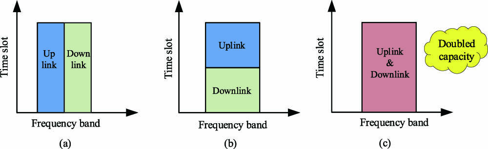
In-band full-duplex (IBFD) technology can double the spectrum utilization efficiency for wireless communications, and increase the data transmission rate of B5G and 6G networks and satellite communications. RF self-interference is the major challenge for the application of IBFD technology, which must be resolved. Compared with the conventional electronic method, the photonic self-interference cancellation (PSIC) technique has the advantages of wide bandwidth, high amplitude and time delay tuning precision, and immunity to electromagnetic interference. Integrating the PSIC system on chip can effectively reduce the size, weight, and power consumption and meet the application requirement, especially for mobile terminals and small satellite payloads. In this paper, the silicon integrated PSIC chip is presented first and demonstrated for IBFD communication. The integrated PSIC chip comprises function units including phase modulation, time delay and amplitude tuning, sideband filtering, and photodetection, which complete the matching conditions for RF self-interference cancellation. Over the wide frequency range of C, X, Ku, and K bands, from 5 GHz to 25 GHz, a cancellation depth of more than 20 dB is achieved with the narrowest bandwidth of 140 MHz. A maximum bandwidth of 630 MHz is obtained at a center frequency of 10 GHz. The full-duplex communication experiment at Ku-band by using the PSIC chip is carried out. Cancellation depths of 24.9 dB and 26.6 dB are measured for a bandwidth of 100 MHz at central frequencies of 12.4 GHz and 14.2 GHz, respectively, and the signal of interest (SOI) with 16-quadrature amplitude modulation is recovered successfully. The factors affecting the cancellation depth and maximum interference to the SOI ratio are investigated in detail. The performances of the integrated PSIC system including link gain, noise figure, receiving sensitivity, and spurious free dynamic range are characterized.
Photonics Research
2023, 11(10): 1635
Author Affiliations
Abstract
School of Optoelectronic Engineering and Instrumentation Science, Dalian University of Technology, Dalian 116024, China
Radio frequency (RF) self-interference is a key issue for the application of in-band full-duplex communication in beyond fifth generation and sixth generation communications. Compared with electronic technology, photonic technology has the advantages of wide bandwidth and high tuning precision, exhibiting great potential to realize high interference cancellation depth over broad band. In this paper, a comprehensive overview of photonic enabled RF self-interference cancellation (SIC) is presented. The operation principle of photonic RF SIC is introduced, and the advances in implementing photonic RF SIC according to the realization mechanism of phase reversal are summarized. For further realistic applications, the multipath RF SIC and the integrated photonic RF SIC are also surveyed. Finally, the challenges and opportunities of photonic RF SIC technology are discussed.
in-band full-duplex radio frequency self-interference cancellation microwave photonics Chinese Optics Letters
2021, 19(7): 073901
1 大连理工大学 光电工程与仪器科学学院, 辽宁 大连 116024
2 大连工业大学 基础教学部, 辽宁 大连 116034
基于狭缝波导结构, 设计了工作波长在890 nm的聚合物基微环。从折射率传感的角度详细分析了狭缝波导的模场特性。分析了波导高度、宽度及狭缝宽度对灵敏度的影响。传统的狭缝波导具有较高的弯曲损耗, 这会影响微环谐振器的品质因子Q以及消光比。设计了非对称的狭缝结构, 保证波导模式位于波导中央传输, 降低弯曲损耗。为了条形波导与狭缝波导更好的耦合, 设计了基于多模干涉结构的条形-狭缝波导模式转换器。仿真表明设计的微环谐振器的传感灵敏度达到109 nm/RIU。
集成光学 狭缝波导 聚合物微环 光学传感 integrated optics slot waveguide polymeric microring optical sensing 红外与激光工程
2020, 49(1): 0118001
大连理工大学光电工程与仪器科学学院, 辽宁 大连 116024
设计了面向Ka频段(30 GHz)相控阵天线的4阵元子阵集成波导光延时网络。该光延时网络采用相位调制方式将射频信号转换至光域,波导微环处于反谐振状态,以实现大带宽、连续可调延时;通过带通滤波仅对一个边带进行延时调控,基于差分平衡探测器还原出射频信号。优化设计了级联双波导微环的结构参数,使每条路径的延时量在0~24.9 ps范围内连续可调,延时带宽大于4 GHz,实现了最大扫描角为±30°的波束扫描。对光延时网络链路的增益和噪声系数进行了推导分析,评估了整个延时芯片系统在实际应用中的性能。
集成光学 光控波束 光延时线 波导微环 反谐振
Author Affiliations
Abstract
1 School of Physics and Optoelectronic Engineering, Dalian University of Technology, Dalian, 116024, China
2 Photonics Research Group, Department of Information Technology, Ghent University-IMEC, 9000 Ghent, Belgium
3 No. 38 Research Institute, China Electronics Technology Group Corporation, Hefei, 230088, China
4 Technical Institute of Physics and Chemistry, Chinese Academy of Sciences, Beijing, 100190, China
The polymer waveguide optical biosensor based on the Mach-Zehnder interferometer (MZI) by using spectral splitting effect is investigated. The MZI based biosensor has two unequal width sensing arms. With the different mode dispersion responses of the two-arm waveguides to the cladding refractive index change, the spectral splitting effect of the output interference spectrum is obtained, inducing a very high sensitivity. The influence of the different mode dispersions between the two-arm waveguides on the spectral splitting characteristic is analyzed. By choosing different lengths of the two unequal width sensing arms, the initial dip wavelength of the interference spectrum and the spectral splitting range can be controlled flexibly. The polymer waveguide optical biosensor is designed, and its sensing property is analyzed. The results show that the sensitivity of the polymer waveguide optical biosensor by using spectral splitting effect is as high as 104 nm/RIU, with an improvement of 2–3 orders of magnitude compared with the slot waveguide based microring biosensor.
Optical biosensor Optical biosensor integrated waveguide integrated waveguide spectral splitting spectral splitting sensitivity sensitivity Photonic Sensors
2017, 7(2): 131–139
Author Affiliations
Abstract
1 School of Physics and Optoelectronic Engineering, Dalian University of Technology, Dalian, 116024, China
2 No. 38 Research Institute, China Electronics Technology Group Corporation, Hefei, 230088, China
3 School of Chemical Engineering, Dalian University of Technology, Dalian, 116024, China
4 Photonics Research Group, Department of Information Technology, Ghent University-IMEC, 9000 Ghent, Belgium
A 2×2 optical waveguide coupler at 850 nm based on the multimode interference (MMI) structure with the polysilsesquioxanes liquid series (PSQ-Ls) polymer material and the imprint technique is presented. The influence of the structural parameters, such as the single mode condition, the waveguide spacing of input/output ports, and the width and length of the multimode waveguide, on the optical splitting performance including the excess loss and the uniformity is simulated by the beam propagation method. By inserting a taper section of isosceles trapezoid between the single mode and multimode waveguides, the optimized structural parameters for low excess loss and high uniformity are obtained with the excess loss of -0.040 dB and the uniformity of -0.007 dB. The effect of the structure deviations induced during the imprint process on the optical splitting performance at different residual layer thicknesses is also investigated. The analysis results provide useful instructions for the waveguide device fabrication.
Polymer waveguide coupler multimode interference Photonic Sensors
2016, 6(3): 234
1 大连理工大学物理与光电工程学院, 辽宁 大连 116024
2 中国电子科技集团第三十八研究所, 安徽 合肥 230088
3 大连理工大学化工学院, 辽宁 大连 116024
Slot结构在提高集成波导光学传感器灵敏度和降低探测极限值方面具有极大的优势。对基于Slot结构的聚合物PSQ-Ls 波导微环光学生物传感器进行了研究。分析了850 nm 波段Slot波导的单波导高度、狭缝宽度及单波导宽度对传感器灵敏度的影响,在满足单模传输的条件下,得到了优化的微环传感器横截面尺寸参数。对Slot结构波导微环的弯曲损耗、自由光谱范围等进行了仿真分析,得到微环传感器的消光比、品质因子等随结构参数的变化,确定了优化的微环弯曲半径、耦合效率。与正脊形结构波导微环传感器相比,Slot结构波导微环传感器的灵敏度是前者的两倍,探测极限值是其一半。
集成光学 Slot波导 波导微环 光学生物传感器 探测极限
1 大连理工大学物理与光电工程学院, 辽宁 大连 116024
2 大连理工大学生命科学与技术学院, 辽宁 大连 116024
3 大连理工大学化工学院, 辽宁大 连 116024
4 中国电子科技集团公司第三十八研究所, 安徽 合肥 230088
温度敏感性是影响波导微环光学生化传感器性能的重要因素。从微环谐振方程出发分析了微环传感器温度敏感性产生的机理,研究了以SU8-NOA61-SU8 三明治结构聚合物衬底代替传统硅衬底,利用衬底的热膨胀效应抵消波导的热光效应,来消除聚合物波导微环光学生化传感器的温度敏感性。采用ANSYS软件对三明治衬底的厚度进行了仿真设计,得到了温度不敏感条件下的衬底厚度参数。对SU8 和NOA61 旋涂成膜工艺进行了实验研究,得到SU8和NOA61的膜厚控制精度分别为0.07 μm@20 r/min 和0.34 μm@20 r/min。分析得到三明治聚合物衬底波导微环传感器的温度敏感性和探测极限值,达到了带有温控装置的硅衬底聚合物波导微环传感器的性能。
集成光学 聚合物波导 微环 光学生化传感器 温度敏感性 光学学报
2015, 35(11): 1113004


